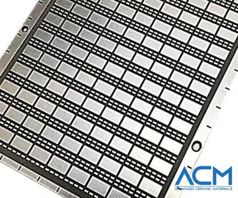
MC6504 Palladium-Gold Plated Alumina PCB
- Catalog No. MC6504
- Material Gold, Palladium, Alumina
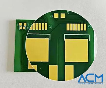
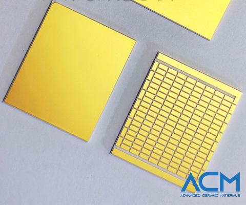
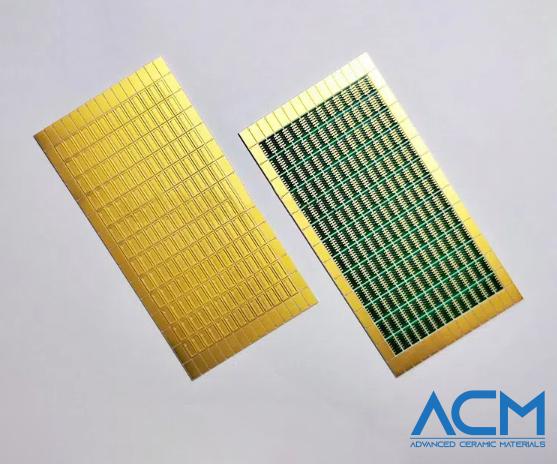
- Appearance Green and Golden Plate
- Thickness 2.0 mm
Inquiry
MC6504 Palladium-Gold Plated Alumina PCB
Description
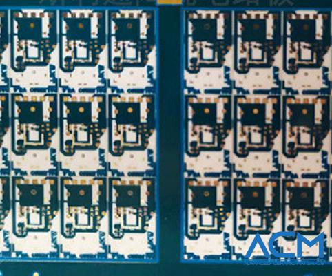
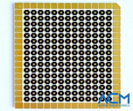
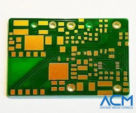
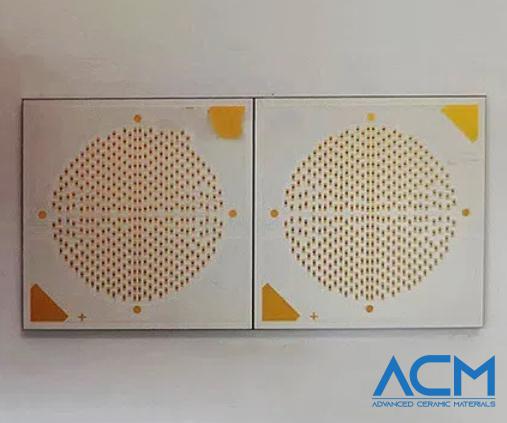
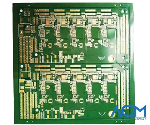
The Palladium-Gold Plated Alumina PCB is a top-tier ceramic circuit board designed to meet the rigorous demands of high-performance electronic systems. Featuring a substantial 2.0mm thick alumina substrate, it delivers excellent thermal conductivity and superior electrical insulation. The multi-layer palladium-gold plating process not only boosts corrosion resistance but also enhances solderability and wire bonding, ensuring robust and reliable connections. Coupled with a green solder mask, this PCB offers additional protection against environmental factors, making it exceptionally durable for use in power electronics, semiconductor devices, and high-frequency applications. Its reliability and long-term stability make it a preferred choice for systems operating in challenging and harsh conditions.
Specifications
| Parameter | Details |
|---|---|
| Materials | Gold, Palladium, Alumina |
| Color/Appearance | Green and Golden Plate |
| Thickness | 2.0 mm |
| Number of Layers | Double-sided |
| Substrate Type | Alumina |
| Copper Plate Thickness | 65 µm |
| Solder Resist | Green Oil |
| Surface Treatment | Immersion Nickel-Palladium |
| Processing | Waterjet Cutting |
| Special Processes | Copper overlay metallization of thick plates, Exterior cutting |
Applications
The Palladium-Gold Plated Alumina PCB is versatile and essential in a variety of high-performance applications, including:
-
Power Electronics
- Uses: Power modules, converters, and inverters
- Benefits: Superior thermal dissipation and electrical insulation ensure efficient and stable operation.
-
Semiconductor Devices
- Uses: Chip carriers, integrated circuits, and high-performance semiconductors
- Benefits: Enhanced corrosion resistance and improved solderability support reliable semiconductor performance.
-
RF Circuits
- Uses: Radio frequency modules, antennas, and communication devices
- Benefits: Maintains signal integrity and stability in high-frequency environments.
-
Telecommunications
- Uses: Base stations, signal processing units, and networking equipment
- Benefits: Ensures consistent performance and durability in high-demand communication systems.
-
Automotive Electronics
- Uses: Advanced Driver Assistance Systems (ADAS), electric vehicle components, and automotive power systems
- Benefits: Robust thermal and electrical properties cater to the demanding automotive environment.
-
Industrial Systems
- Uses: High-power industrial controllers, automation systems, and machinery
- Benefits: Ensures efficient thermal management and long-term reliability in industrial settings.
Packaging
Our Palladium-Gold Plated Alumina PCBs are meticulously handled during storage and transportation to maintain their integrity and quality. Each PCB is securely packaged to prevent any damage, ensuring that it arrives at your location in pristine condition, ready for integration into your high-performance electronic systems.
Frequently Asked Questions (FAQ)
Q1: What is a Palladium-Gold Plated Alumina PCB?
A1: The Palladium-Gold Plated Alumina PCB is a high-performance ceramic circuit board made from a 2.0mm thick alumina substrate. It features a multi-layer palladium-gold plating that enhances thermal conductivity, electrical insulation, corrosion resistance, solderability, and wire bonding capabilities. The green solder mask provides additional protection, making it suitable for demanding electronic applications.
Q2: What are the advantages of using this PCB?
A2:
- Superior Thermal Conductivity: Efficient heat dissipation ensures optimal performance in high-power applications.
- Excellent Electrical Insulation: Provides reliable electrical isolation for stable operation.
- Enhanced Corrosion Resistance: Prolongs the lifespan of the PCB in harsh environments.
- Improved Solderability and Wire Bonding: Facilitates secure and efficient connections.
- Durable Solder Mask: Protects the circuitry, ensuring long-term reliability and stability.
Q3: What are the typical applications for this PCB?
A3:
- Power Electronics: Power modules, converters, and inverters.
- Semiconductor Devices: Chip carriers and integrated circuits.
- RF Circuits: Radio frequency modules and antennas.
- Telecommunications: Base stations and networking equipment.
- Automotive Electronics: ADAS and electric vehicle components.
- Industrial Systems: High-power controllers and automation systems.
Request a Quote
-
Attachment (Optional)
No file chosen


