


Difference Between Prime & Research Grade Silicon Carbide Wafers
Introduction
Silicon Carbide (SiC) wafers stand at the forefront of semiconductor technology, offering unparalleled efficiency and performance for a wide range of applications, from power electronics to renewable energy systems. The decision between Prime and Research grade SiC wafers hinges on balancing performance requirements against cost, where each grade serves distinct needs—Prime for high-end applications demanding the utmost reliability and Research for exploratory projects and applications with more flexibility in performance criteria. This guide delves into the critical aspects of SiC wafers, aiding customers in navigating the selection process to match their specific project demands.
Here is a QUICK GUIDE for this article:
- Understanding SiC Wafers
- Grade Selection Criteria for SiC Wafers
- Prime Grade SiC Wafers
- Research Grade SiC Wafers
- Direct Comparison for Decision-Making
- Conclusion and Buying Tips
Understanding SiC Wafers
Silicon Carbide (SiC) is renowned for its exceptional material properties that cater to advanced semiconductor applications, fundamentally altering the landscape of power electronics and photonics. At their core, SiC wafers exhibit superior thermal conductivity, allowing devices to operate at higher temperatures without compromising performance. This characteristic is pivotal for power devices in electric vehicles and industrial systems, where efficiency and durability under thermal stress are paramount.
Additionally, SiC's wide bandgap energy enables the creation of devices that can operate at higher voltages and frequencies, significantly enhancing energy efficiency and reducing size and weight compared to silicon-based counterparts. This wide bandgap also contributes to SiC devices' ability to offer greater power densities, a critical factor in applications from renewable energy converters to high-speed, high-frequency communication systems.
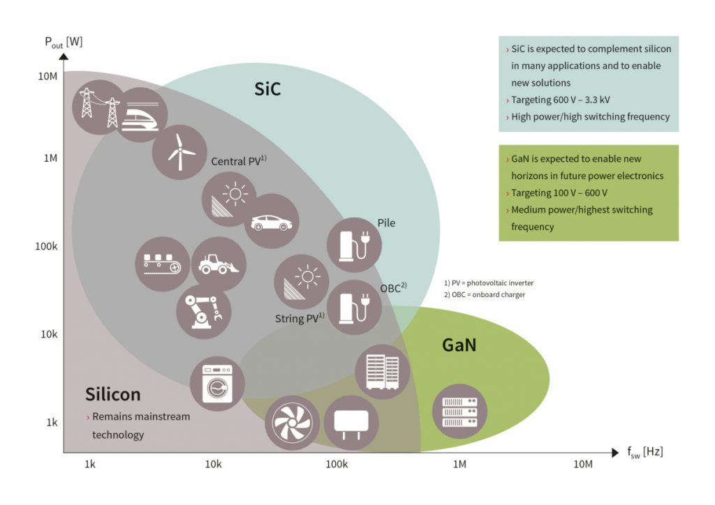
Wide Bandgap Semiconductors
The mechanical robustness of SiC further ensures reliability and longevity in harsh environments, making it suitable for demanding applications in aerospace, defense, and beyond. The choice of grade—Prime or Research—directly influences these properties, with each grade tailored to meet specific performance thresholds and cost considerations. Understanding the intrinsic properties of SiC wafers and the impact of grade selection is crucial for engineers and designers to harness the full potential of this material in their innovations.
Grade Selection Criteria for SiC Wafers
The grading of Silicon Carbide (SiC) wafers is determined by several key criteria that directly influence their suitability for various applications, ensuring that the chosen wafers align with the specific requirements of the devices being developed. Among the foremost considerations are defect density and electrical properties, which are critical to the performance and reliability of SiC-based components.
Defect Density: A primary factor in grading SiC wafers, defect density includes micropipe densities and dislocations. Prime grade wafers exhibit significantly lower defect densities, essential for high-performance applications where even minimal imperfections could lead to failure or reduced efficiency. Research grade wafers, while having higher defect densities, are suitable for experimental applications or non-critical components where slight imperfections are tolerable.
Electrical Properties: The uniformity and specific characteristics of electrical properties such as doping concentration and carrier mobility are crucial. Prime grade wafers offer tight control over these properties, ensuring consistent device performance. Research grade wafers may exhibit wider variability, making them ideal for applications where such precision is less critical.
Prime Grade SiC Wafers
Prime Grade Silicon Carbide (SiC) wafers represent the pinnacle of quality within the semiconductor industry, designed for applications where superior performance and reliability are non-negotiable. Characterized by a useable area of greater than or equal to 90%, these wafers have an impressively low defect density, with micropipe densities (MPD) of less than or equal to 5/cm^2, ensuring minimal imperfections that could impair device functionality. Additionally, they exhibit resistivity uniformity of greater than or equal to 90%, which is critical for applications requiring consistent electrical performance across the wafer.
Table 1. Specification of Prime Grade SiC Wafers
| Specification | Value |
|---|---|
| Useable Area | >=90% |
| Defect Density (MPD) | <=5/cm^2 |
| Resistivity Uniformity | >=90% |
| Thickness, Warp & Bow | Best |
| Surface Defects | No |
The prime grade also boasts the best values in terms of thickness, warp, and bow, attributes that contribute to the stability and efficacy of the end semiconductor device. The absence of surface defects further underscores their suitability for high-end applications. This meticulous attention to quality makes Prime Grade wafers the necessary choice for critical applications in power electronics, such as electric vehicle powertrains, renewable energy power converters, high-performance computing, and military or aerospace technologies where failure is not an option.
Research Grade SiC Wafers
Research Grade SiC wafers, while still maintaining a high standard of quality, are tailored for cost-effectiveness and suitability for experimentation and less critical applications. These wafers offer a useable area of greater than or equal to 80% and tolerate a higher defect density with micropipe densities (MPD) of less than or equal to 10/cm^2. Such specifications make them particularly well-suited for academic research, prototype development, and applications where the absolute highest performance metrics may be compromised for cost savings.
Table 2. Specification of Research Grade SiC Wafers
| Specification | Value |
|---|---|
| Useable Area | >=80% |
| Defect Density (MPD) | <=10/cm^2 |
| Resistivity Uniformity | >=80% |
| Thickness, Warp & Bow | Better |
| Surface Defects | Very few and small |
With resistivity uniformity of greater than or equal to 80% and better (though not optimal) thickness, warp, and bow values, Research Grade wafers provide a viable platform for a wide array of experimental and developmental projects. The presence of very few and small surface defects does not significantly impact applications that can tolerate minor inconsistencies, such as initial stage research or educational purposes. This grade is ideal for organizations looking to push the boundaries of SiC technology through innovative experimentation or for those developing products where the utmost in performance is not critical, enabling cost savings and flexibility in design and application.
Direct Comparison for Decision Making: Prime vs. Research Grade SiC Wafers
When selecting Silicon Carbide (SiC) wafers for semiconductor applications, understanding the nuanced differences between Prime and Research grades is crucial. This comparison not only illuminates the distinct advantages of each but also aids in aligning with potential customer concerns such as performance, cost, and application specificity.
Silicon Carbide Wafer
Performance: Prime grade SiC wafers stand out for their exceptional performance, characterized by higher purity, lower defect densities, and greater uniformity in electrical properties. These characteristics are pivotal for applications where superior device reliability, efficiency, and longevity are critical. For instance, in power electronics for electric vehicles (EVs) or in aerospace applications, where failure could have significant safety implications, Prime grade wafers are indispensable. Their superior thermal and electrical performance ensures devices operate effectively under high stress and temperature conditions.
Conversely, Research grade wafers, while still maintaining a high level of quality, have slightly higher defect densities and variability in properties. This grade is perfectly suited for research and development environments, where the focus is on exploring new designs and technologies rather than mass production. Research grade wafers offer a cost-effective solution for universities and R&D departments working on next-generation semiconductors, where some variability can be accommodated within the experimental parameters.
Cost: The advanced manufacturing processes and stringent quality controls required to produce Prime grade SiC wafers reflect in their cost. These wafers are priced higher due to their enhanced properties and the value they bring to critical applications. In contrast, Research grade wafers are more affordably priced, making them an attractive option for experimental projects and applications where budget constraints are a significant consideration.
Application Specificity: Choosing the right grade depends heavily on the application's specific requirements. For high-performance, commercial, and safety-critical applications, the investment in Prime grade wafers is justified by the need for utmost reliability and performance. For example, in the production of power modules for EVs, the high thermal conductivity and low defect density of Prime grade wafers can significantly enhance the vehicle's range and efficiency.
In academic or exploratory settings, where the focus is on innovation rather than immediate commercial viability, Research grade wafers provide a practical platform. These wafers are ideal for applications such as prototyping new semiconductor devices or conducting fundamental material science studies, where slight imperfections do not impede the project's goals.
Case Scenarios:
High-Performance Computing: A manufacturer developing silicon carbide-based chips for high-performance computing systems would opt for Prime grade wafers to ensure the highest efficiency and thermal management capabilities, given the chips' application in data centers where operational uptime and performance are critical.
Academic Research: A university research team exploring novel SiC semiconductor structures for potential use in renewable energy systems may choose Research grade wafers. The slightly higher defect density is a reasonable trade-off for the lower cost, especially when the research focuses on theoretical performance improvements or material characteristics.
Decision Making
The decision between Prime and Research grade SiC wafers hinges on balancing several factors: the performance requirements of the end application, cost considerations, and the specific needs of the project. Prime grade wafers are essential for applications demanding the highest reliability and performance, whereas Research grade wafers offer a cost-effective solution for experimental and non-critical applications. By carefully considering these factors, customers can make informed decisions that align with their project's goals and budget constraints, ensuring the successful implementation of SiC technology in their applications.
Table 3. Decision Making between Prime vs. Research Grade SiC Wafers
| Specification | Prime Grade Value | Research Grade Value |
|---|---|---|
| Useable Area | >=90% | >=80% |
| Defect Density (MPD) | <=5/cm^2 | <=10/cm^2 |
| Resistivity Uniformity | >=90% | >=80% |
| Thickness, Warp & Bow | Best | Better |
| Surface Defects | No | Very few and small |
Table 4. Specification Difference between Prime vs. Research Grade SiC Wafers
| Criteria | Prime Grade | Research Grade |
|---|---|---|
| Defect DensityDefect Density | Lower defects; crucial for high-performance. | Higher defects; fits experimental use. |
| Electrical Properties | Consistent electrical performance. | Variable electrical properties; suits non-critical applications. |
| Cost | Higher, due to stringent quality. | More affordable, suitable for R&D. |
| Application | Suitable for high-performance, critical applications. | Ideal for prototypes, academic research. |
| Use Cases | EV power modules, high-performance computing. | Prototyping, material studies. |
Conclusion and Buying Tips
Selecting the right grade of Silicon Carbide (SiC) wafers is pivotal for the success of semiconductor projects, with Prime and Research grades catering to distinct needs. Prime Grade wafers are indispensable for applications demanding the highest performance and reliability, such as in power electronics and aerospace, where their superior purity and lower defect densities ensure optimal functionality. Research Grade wafers, offering a balance between quality and cost, are ideal for experimental and developmental projects, where flexibility in specifications can foster innovation.
When making a purchase decision, consider the specific requirements of your application, including performance expectations and budget constraints. Evaluate the vendor's reputation, quality assurance processes, and the ability to provide technical support. Advanced Ceramic Materials (ACM) stands out as a reliable supplier of both Prime and Research Grade SiC wafers, offering extensive expertise and customer service to guide you through the selection process.
Ultimately, the choice between Prime and Research grade should align with your project's goals, leveraging the unique advantages of each to meet your application's demands. Careful consideration of wafer specifications and vendor capabilities will ensure you make the most informed decision, positioning your semiconductor project for success.
{{item.content}}
LEVE A REPLY
{{item.children[0].content}}
{{item.content}}
LEAVE A REPLY
SUBSCRIBE OUR NEWSLETTER
- Oxide, Sulfide, or Phosphate? A Supplier's Guide to Solid-State Electrolyte Ceramics
- Alumina vs. Zirconia Ceramics: The Engineering Blueprint for Material Selection
- Case Study: Sub-Millimeter Sapphire Tubes for High Voltage Discharge Applications
- Alumina Powder (Al2O3): A Technical Guide to Grades, Properties, and Applications
- Ceramic Machining: Essential Techniques and Processes for Precise Components
 Alumina Powder (Al2O3): A Technical Guide to Grades, Properties, and Applications
How to choose alumina powder purity from 92% to 99.99%. ACM guide covers decision tree, properties, ZTA, and application tables for engineers.
READ MORE >
Alumina Powder (Al2O3): A Technical Guide to Grades, Properties, and Applications
How to choose alumina powder purity from 92% to 99.99%. ACM guide covers decision tree, properties, ZTA, and application tables for engineers.
READ MORE >
 Alumina vs. Zirconia Ceramics: The Engineering Blueprint for Material Selection
This article compares their physical properties, real-world trade-offs, and cost-benefit realities to help you select the right ceramic for your operating environment.
READ MORE >
Alumina vs. Zirconia Ceramics: The Engineering Blueprint for Material Selection
This article compares their physical properties, real-world trade-offs, and cost-benefit realities to help you select the right ceramic for your operating environment.
READ MORE >
 Oxide, Sulfide, or Phosphate? A Supplier's Guide to Solid-State Electrolyte Ceramics
Oxide, sulfide, or phosphate? A practical guide to solid-state electrolyte ceramics from a supplier who handles them daily. Compare LLZO, LATP, and LGPS on conductivity, processing, stability, and real-world viability.
READ MORE >
Oxide, Sulfide, or Phosphate? A Supplier's Guide to Solid-State Electrolyte Ceramics
Oxide, sulfide, or phosphate? A practical guide to solid-state electrolyte ceramics from a supplier who handles them daily. Compare LLZO, LATP, and LGPS on conductivity, processing, stability, and real-world viability.
READ MORE >