


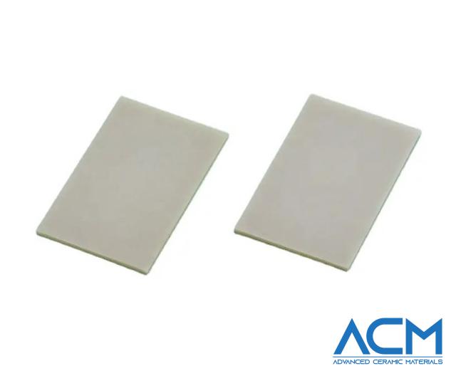
AlN Ceramic Substrates for UV-LED and Mini LED Packaging
Thermal management in LED packaging rarely follows a single pattern. A UV-LED curing system might concentrate 50 W into a 1 mm² emitter, while a Mini LED display spreads the same total power across thousands of microscopic sites. Different problems—but they lead to the same material conclusion. In both cases, the substrate needs thermal conductivity above 170 W/mK to keep junction temperatures under control, and a CTE that moves with the semiconductor rather than fighting it. Aluminum nitride consistently meets those requirements. The question is how to select the right metallization and format for your specific packaging approach.
1. Thermal Demands in Current LED Architectures
In UV-LEDs operating below 365 nm, wall-plug efficiency typically ranges from 30% to 40%. The remaining 60-70% of input power dissipates as heat within a package often measuring less than 2 mm². Without adequate heat spreading, junction temperatures rise rapidly. For every 10°C increase above rated operating temperature, median device lifetime decreases by approximately 50% in typical GaN-based UV emitters.
Mini LED arrays present a different thermal profile. Individual chips operate at moderate power densities, but array densities reaching 10,000-15,000 emitters per panel create cumulative heat fluxes that conventional substrates cannot manage uniformly. Temperature gradients across the panel translate directly into chromaticity shifts and visible brightness variation. Maintaining junction temperature variation below 5°C across the array requires in-plane thermal spreading capabilities that standard PCB materials do not provide.
Both cases share a common requirement: the substrate must function as an active thermal management component, not merely a mechanical carrier.
2. Substrate Material Comparison
The progression from FR4 to metal core PCBs to alumina and finally to Aluminum nitride (AlN) reflects increasing thermal demands in LED packaging. Each material class has fundamental limitations:
| Material | Thermal Conductivity (W/mK) | CTE (ppm/K) | Primary Limitation |
|---|---|---|---|
| FR4 | 0.3-0.4 | 14-17 | Decomposes above 130°C |
| Metal Core PCB | 1-3 (through dielectric) | ~23 (Al base) | Dielectric layer limits effective conductivity |
| Alumina (Al₂O₃) | 20-30 | 6.5-7.0 | Insufficient for >50 W/cm² heat flux |
| Aluminum Nitride (AlN) | 140-230 | 4.5-4.7 | Higher material cost |
AlN's thermal conductivity approaches that of aluminum metal (237 W/mK) while maintaining electrical resistivity >10¹⁴ Ω·cm. Its CTE of 4.5-4.7 ppm/K provides an intermediate match between silicon (2.6 ppm/K), gallium nitride (3.2-5.6 ppm/K), and the surrounding package materials. For UV applications, AlN's wide bandgap (6.2 eV) renders it transparent to wavelengths above 200 nm, eliminating the photon degradation observed in polymer-based substrates.

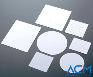
3. Metallization Methods for Different Packaging Formats
AlN requires metallization to form circuit patterns. The choice of metallization method depends on current requirements, feature density, and assembly process.
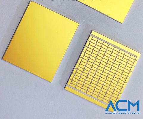
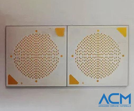
Direct Plate Copper (DPC)
A copper foil (100-300 µm) is bonded to the AlN surface at elevated temperature, then photolithographically patterned. This method suits Chip-on-Board (COB) configurations requiring high current capacity and lateral heat spreading. The bond interface quality is critical: void fractions below 5% with maximum unbonded area under 2% are necessary to prevent hot spots. Thermal conductivity across the bond line typically exceeds 200 W/mK when properly processed.
Thin Film Metallization
For Mini LED arrays requiring fine-pitch interconnects, sputtered titanium adhesion layers followed by copper plating produce line/space resolutions down to 20 µm. Metal thickness ranges from 1-10 µm, sufficient for signal transmission but not for high-current distribution. Surface roughness below 0.1 µm Ra is achievable with this method.
Surface Finishes for Assembly
For eutectic die attach, electroless nickel immersion gold (ENIG) provides a solderable surface with good wetting characteristics. For silver sintering applications, direct silver plating offers the lowest thermal resistance interface. The finish selection should precede substrate specification, as different finishes require different base metallization thicknesses and processing parameters.
4. Reliability Data Under Accelerated Testing
Accelerated life testing provides a basis for comparing substrate performance. The following data represents average results from 50-unit samples of AlN-based LED modules tested at Advanced Ceramic Materials' laboratory.
Test Conditions:
-
Ambient temperature: 85°C
-
Relative humidity: 85%
-
Duration: 1000 hours
-
Current: Rated continuous
Results:
| Parameter | Initial | 1000 Hours | Change |
|---|---|---|---|
| Luminous flux (relative) | 1.00 | 0.96 | -4% |
| Forward voltage (V_f) | 3.22 | 3.18 | -1.2% |
| Insulation resistance (Ω) | >10¹² | >10¹¹ | — |
| Solder joint resistance (mΩ) | 2.1 | 2.3 | +9.5% |
The 4% flux degradation falls within typical expectations for InGaN LEDs under these conditions. Forward voltage stability indicates minimal contact degradation. Solder joint resistance increase of 9.5% reflects some intermetallic growth but remains below failure thresholds.
For comparison, identical LED packages assembled on alumina substrates under the same conditions showed 15-18% flux degradation and 25-30% solder joint resistance increase over 1000 hours.
5. Substrate Selection Guidelines
Based on the data presented, the following selection criteria apply:
For UV-LEDs >100 mW/mm²:
-
Specify AlN with thermal conductivity ≥180 W/mK
-
Use DPC metallization with copper thickness ≥150 µm
-
Require bond quality documentation showing >95% bonded area
-
Select Ag or AuSn-compatible finishes for eutectic attach
For Mini LED arrays with pitch <200 µm:
-
Specify AlN with thermal conductivity ≥170 W/mK
-
Use thin film metallization with line/space resolution matching array density
-
Verify surface planarity within ±10 µm across the panel
-
Require lot traceability for CTE uniformity
For hybrid applications requiring both:
-
Consider multilayer AlN substrates with embedded vias
-
Specify matched CTE between layers
-
Verify dielectric breakdown voltage >2 kV for series configurations
Summary
AlN ceramic substrates address the thermal limitations of FR4, metal core, and alumina alternatives in high-density and high-flux LED applications. Thermal conductivity exceeding 170 W/mK combined with CTE matching to semiconductor materials enables junction temperature control within design targets. Metallization options including DPC and thin film methods accommodate both high-current and fine-pitch configurations. Accelerated test data confirms reliability improvements over conventional substrate materials under 85°C/85%RH conditions.
For substrate specifications tailored to your application:
Advanced Ceramic Materials (ACM) maintains a range of aluminum nitride ceramic grades and metallization options qualified for LED packaging. If you're working through a thermal design or comparing substrate options, we are available to review your requirements.
{{item.content}}
LEVE A REPLY
{{item.children[0].content}}
{{item.content}}
LEAVE A REPLY
SUBSCRIBE OUR NEWSLETTER
- Oxide, Sulfide, or Phosphate? A Supplier's Guide to Solid-State Electrolyte Ceramics
- Alumina vs. Zirconia Ceramics: The Engineering Blueprint for Material Selection
- Case Study: Sub-Millimeter Sapphire Tubes for High Voltage Discharge Applications
- Alumina Powder (Al2O3): A Technical Guide to Grades, Properties, and Applications
- Ceramic Machining: Essential Techniques and Processes for Precise Components
 Alumina Powder (Al2O3): A Technical Guide to Grades, Properties, and Applications
How to choose alumina powder purity from 92% to 99.99%. ACM guide covers decision tree, properties, ZTA, and application tables for engineers.
READ MORE >
Alumina Powder (Al2O3): A Technical Guide to Grades, Properties, and Applications
How to choose alumina powder purity from 92% to 99.99%. ACM guide covers decision tree, properties, ZTA, and application tables for engineers.
READ MORE >
 Alumina vs. Zirconia Ceramics: The Engineering Blueprint for Material Selection
This article compares their physical properties, real-world trade-offs, and cost-benefit realities to help you select the right ceramic for your operating environment.
READ MORE >
Alumina vs. Zirconia Ceramics: The Engineering Blueprint for Material Selection
This article compares their physical properties, real-world trade-offs, and cost-benefit realities to help you select the right ceramic for your operating environment.
READ MORE >
 Oxide, Sulfide, or Phosphate? A Supplier's Guide to Solid-State Electrolyte Ceramics
Oxide, sulfide, or phosphate? A practical guide to solid-state electrolyte ceramics from a supplier who handles them daily. Compare LLZO, LATP, and LGPS on conductivity, processing, stability, and real-world viability.
READ MORE >
Oxide, Sulfide, or Phosphate? A Supplier's Guide to Solid-State Electrolyte Ceramics
Oxide, sulfide, or phosphate? A practical guide to solid-state electrolyte ceramics from a supplier who handles them daily. Compare LLZO, LATP, and LGPS on conductivity, processing, stability, and real-world viability.
READ MORE >