


The Amor of Semiconductor Tools: Why High-Purity Al2O3 & AlN Are Preferred for Plasma Process Chambers
In the high-stakes environment of semiconductor manufacturing, plasma process chambers are battlegrounds of extreme chemistry and physics. The ceramic components lining these chambers—showerheads, liners, focus rings—must withstand relentless attack. This article explores why high-purity Aluminum Oxide (Al2O3) and Aluminum Nitride (AlN) have become the materials of choice, comparing their performance in critical areas like plasma corrosion resistance, metal contamination control, and thermal management. We delve into application-specific requirements and outline what fabricators should demand from their ceramic component supplier to maximize uptime and yield.
Introduction: The Frontline Defense in Fab
A single particle or trace metal contaminant in a plasma etch, or chemical vapor deposition (CVD) chamber can spell disaster, leading to wafer defects, tool downtime, and millions in lost revenue. The interior components of these chambers act as the first line of defense. They are not passive liners but active participants in the process, subject to intense ion bombardment, corrosive chemistries (Cl₂, F-based, O₂), and significant thermal cycling.
Choosing the wrong material accelerates wear, increases particle generation, and introduces unwanted elements into the process stream. This has driven the industry toward advanced technical ceramics, with high-purity Al₂O₃ and AlN emerging as the undisputed champions for most critical applications. Their selection is a calculated decision based on a stringent set of property requirements.
Material Comparison: Al₂O₃ vs. AlN
While both ceramics excel in plasma environments, their unique properties make them suited for slightly different challenges within the chamber.
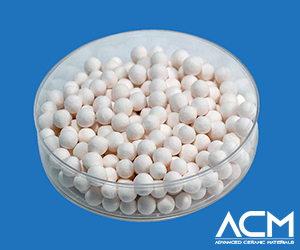
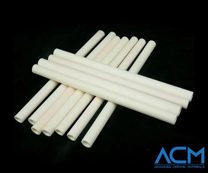
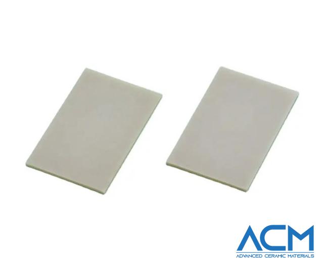
High-Purity Alumina (Al₂O₃ ≥99.6%)
- Plasma Corrosion Resistance: Exhibits excellent resistance to a wide range of process chemistries, particularly in high-ion-density etch applications. Its dense, stable structure provides a long service life against physical and chemical sputtering.
- Metal Contamination Control: Ultra-high purity grades (with total metallic impurities in the low ppm range) ensure minimal risk of introducing mobile ions (like Na⁺, K⁺) or transition metals (Fe, Ni) that could migrate into sensitive device layers.
- Dielectric Strength & Arc Resistance: A superb electrical insulator, it prevents unwanted arcing in RF-driven plasmas, which can cause local melting, particle generation, and process instability.
- Thermal Shock Resistance: While moderate, its performance is sufficient for many applications. However, rapid, large temperature swings remain a challenge.
Aluminum Nitride (AlN)
- Plasma Corrosion Resistance: Generally superior to Al₂O₃ in halogen-based plasmas, offering exceptional stability. However, it can be susceptible to oxidation in oxygen-rich environments at high temperatures.
- Metal Contamination Control: Also available in high-purity forms. Critical control of oxygen content within the AlN matrix is essential, as oxygen can affect both thermal and electrical properties.
- Thermal Conductivity (The Key Differentiator): With a thermal conductivity (~170-220 W/m·K) nearly 10 times that of Al₂O₃, AlN is the material of choice for components requiring active thermal management, such as heated showerheads in CVD or electrostatic chucks (ESCs). This enables superior temperature uniformity across the wafer.
- Thermal Shock Resistance: Its high thermal conductivity, combined with a moderate thermal expansion coefficient, grants AlN outstanding thermal shock resistance, crucial for processes with rapid thermal cycles.

Performance Comparison Table
| Property | High-Purity Al₂O₃ | High-Purity AlN | Key Implication |
|---|---|---|---|
| Plasma Etch Rate | Low | Very Low | Longer component life, fewer PM cycles |
| Thermal Conductivity | ~25-32 W/m·K | ~170-220 W/m·K | AlN enables precise wafer temperature control |
| Dielectric Strength | Excellent | Excellent | Preforms arc suppression in RF applications |
| Primary Cost Driver | Powder purity, sintering | Powder purity, nitridation, post-HIPing | Essential for evaluating supplier capability and achieving the optimal cost/performance balance. |
Application-Specific Demands: Matching Ceramic to Component
Not all chamber parts are created equal. The ideal material and its fabrication must align with the component's function.
Gas Distribution Showerheads:
- Function: Deliver process gases uniformly across the wafer. Often RF-powered and/or heated.
- Material Choice: AlN is typically preferred due to its need for excellent thermal conductivity for heating and temperature uniformity. Requires ultra-fine, clog-resistant hole drilling and metallization for brazing or RF connection.
- Critical Ceramic Traits: High purity, exceptional thermal conductivity uniformity, precise dimensional control for hole patterning.
Chamber Liners & Shields:
- Function: Protect permanent chamber walls from deposition and etch byproducts. Consumable parts replaced during preventive maintenance (PM).
- Material Choice: High-purity Al₂O₃ is the common workhorse, offering an optimal balance of plasma resistance, low cost of ownership, and manufacturability for large, complex shapes.
- Critical Ceramic Traits: High density (>3.90 g/cm³) to minimize porosity and particle shedding, excellent surface finish to reduce adhesion of deposits, and high strength.
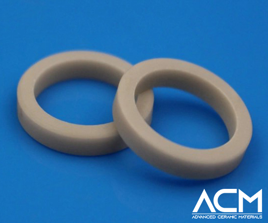
Focus Rings (Edge Rings):
- Function: Control plasma density and uniformity at the wafer edge, critical for etch profile control.
- Material Choice: Can be Al₂O₃, AlN, or Quartz/SiC, depending on the process. Al₂O₃ is common for its etch resistance and dielectric properties.
- Critical Ceramic Traits: Exceptional dimensional stability and wear resistance to maintain precise critical dimensions (CD) over its lifespan. Consistent material properties are key to predictable etch rates.

Insulation Rings & Standoffs:
- Function: Provide electrical and thermal isolation between components.
- Material Choice: Primarily Al₂O₃ for its supreme dielectric strength and cost-effectiveness.
- Critical Ceramic Traits: High dielectric breakdown voltage, low dielectric loss, and mechanical stability under clamp load.
The ACM Advantage: Engineering Ceramics for Extreme Environments
At Advanced Ceramic Materials (ACM), we understand that supplying components for semiconductor equipment is not just about manufacturing ceramics—it's about delivering guaranteed performance under extreme duress. Our process is engineered for this mission:
- Purity at the Core: We start with ≥99.6% Al₂O₃ and high-grade AlN powders, rigorously screened for metallic impurities. Our entire production flow is designed to prevent contamination.
- Uniformity Through Isostatic Pressing: For complex shapes like liners and showerheads, we utilize Cold Isostatic Pressing (CIP) followed by precision machining of the green body. This ensures uniform density throughout the part, eliminating weak zones that could fail in service.
- Density & Strength via HIP: For the most critical components, especially large or complex AlN parts, we employ Hot Isostatic Pressing (HIP) as a post-sintering treatment. This process eliminates residual porosity, pushing density to near-theoretical values (>99.5%), which maximizes mechanical strength, thermal conductivity, and plasma resistance while minimizing particle generation.
- Precision Finishing: We achieve the surface finishes and dimensional tolerances demanded by OEMs, often in the micron range, through advanced grinding and lapping techniques.
Conclusion: A Strategic Partnership for Fab Performance
The ceramic components inside a plasma chamber are vital, wear-prone elements that directly impact tool availability and process yield. Selecting between Al₂O₃ and AlN—and more importantly, selecting a supplier capable of delivering these materials with semiconductor-grade consistency—is a critical technical and business decision.
A partner like ACM provides more than just a ceramic part; we provide a material solution backed by controlled chemistry, advanced forming, and rigorous quality assurance. This translates to longer mean time between failures (MTBF), predictable maintenance schedules, and ultimately, a lower cost of ownership for your fab.
Ready to specify the right ceramic armor for your process tools?
Contact ACM's technical team today to receive our comprehensive guide, which includes detailed property data, application maps, and a supplier qualification checklist tailored for semiconductor equipment manufacturers and end fabs.
{{item.content}}
LEVE A REPLY
{{item.children[0].content}}
{{item.content}}
LEAVE A REPLY
SUBSCRIBE OUR NEWSLETTER
- How PBN Crucibles Ensure the Quality of GaN & SiC Epitaxial Materials
- SiC vs. Quartz Focus Rings: A Cost and Performance Analysis for Advanced Etch
- AlN Ceramic Substrates: Enabling Next-Gen Electrostatic Chucks
- Silicon Carbide - Ultra-High Temperature Ceramics for Extreme Environments
- Aluminum Oxide Ceramics: Properties and Applications
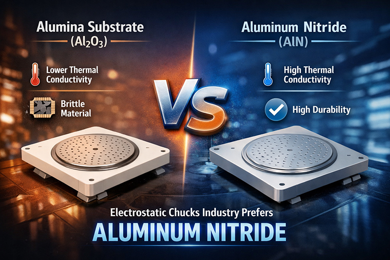 AlN Ceramic Substrates: Enabling Next-Gen Electrostatic Chucks
This article details the material properties forcing this change and provides a framework for ESC builders to evaluate and source the high-performance AlN substrates necessary to win in the advanced node market.
READ MORE >
AlN Ceramic Substrates: Enabling Next-Gen Electrostatic Chucks
This article details the material properties forcing this change and provides a framework for ESC builders to evaluate and source the high-performance AlN substrates necessary to win in the advanced node market.
READ MORE >
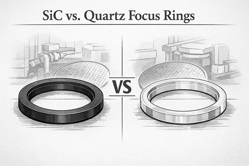 SiC vs. Quartz Focus Rings: A Cost and Performance Analysis for Advanced Etch
Quartz focus rings wear fast in advanced etch, hurting yield. Silicon Carbide (SiC) rings last 6-10x longer. Our TCO analysis shows how SiC's higher price lowers total cost. Get the selection guide and corrosion data.
READ MORE >
SiC vs. Quartz Focus Rings: A Cost and Performance Analysis for Advanced Etch
Quartz focus rings wear fast in advanced etch, hurting yield. Silicon Carbide (SiC) rings last 6-10x longer. Our TCO analysis shows how SiC's higher price lowers total cost. Get the selection guide and corrosion data.
READ MORE >
 How PBN Crucibles Ensure the Quality of GaN & SiC Epitaxial Materials
In the atomic-scale world of GaN HEMTs and SiC power devices, the vessel that holds the source materials is not just a container; it is the foundational determinant of epitaxial film purity. Trace contaminants from a crucible can incorporate as fatal defects. This article details why Pyrolytic Boron Nitride (PBN) has become the non-negotiable material for MOCVD and MBE components, examining its unique combination of ultra-high purity, thermal management, and non-wetting properties.
READ MORE >
How PBN Crucibles Ensure the Quality of GaN & SiC Epitaxial Materials
In the atomic-scale world of GaN HEMTs and SiC power devices, the vessel that holds the source materials is not just a container; it is the foundational determinant of epitaxial film purity. Trace contaminants from a crucible can incorporate as fatal defects. This article details why Pyrolytic Boron Nitride (PBN) has become the non-negotiable material for MOCVD and MBE components, examining its unique combination of ultra-high purity, thermal management, and non-wetting properties.
READ MORE >