


N-Type and Semi-Insulating SiC: Choosing the Right Material for Power and RF Devices
1. Understanding the Role of SiC in Electronics
Silicon carbide (SiC) is known for its wide bandgap, strong thermal stability, and ability to withstand high electric fields. These features make it one of the go-to materials for next-generation electronic components, especially where power density or switching speed is critical.
However, SiC comes in different electrical types. Two common variants—N-type and semi-insulating (SI)—behave very differently, and that matters when designing devices. Knowing when to use each is key to building efficient and reliable systems.

2. Material Basics: What Sets Them Apart?
N-Type SiC
This version contains small amounts of donor impurities, like nitrogen or phosphorus. These atoms introduce extra electrons, allowing current to flow.
-
Carrier type: electrons
-
Resistivity: typically between 0.01 and 10 Ω·cm
-
Mobility: relatively high (~700–1000 cm²/V·s)
It’s conductive and works well in power devices where you want charge to move.
Semi-Insulating SiC
In contrast, SI-SiC is engineered to block current. This is done either by growing ultra-pure crystals or by adding deep-level dopants like vanadium. The goal is to cancel out free carriers and reach high resistivity.
-
Carrier concentration: under 10⁹ cm⁻³
-
Resistivity: above 10⁶ Ω·cm
-
No active conduction path under normal conditions
This type is favored when electrical isolation is more important than conduction.
3. Property Comparison
| Property | N-Type SiC | SI-SiC |
|---|---|---|
| Resistivity | 0.01–10 Ω·cm | >10⁶ Ω·cm |
| Carrier Type | Electrons | None (compensated) |
| Carrier Concentration | 10¹⁶–10¹⁸ cm⁻³ | <10⁹ cm⁻³ |
| Breakdown Field | High | Even higher |
| Electrical Mobility | ~700–1000 cm²/V·s | Not applicable |
These differences impact both device design and system layout, especially in high-voltage and high-frequency domains.
4. Where Each Material Fits
N-Type Use Cases
Because it allows current to flow, N-type SiC is found in:
-
Power switches like MOSFETs, IGBTs, and Schottky diodes
-
Substrates for LED devices
-
Vertical and lateral power modules for electric vehicles, solar inverters, etc.
SI-SiC Use Cases
If the job calls for electrical insulation and high-frequency performance, SI-SiC is a better fit:
-
RF devices like HEMTs and MESFETs
-
High-voltage buffers and isolation layers
-
GaN-on-SiC substrates, especially in telecom and radar systems
The material doesn’t carry current, but supports layers that do—without adding interference.
5. Manufacturing and Cost Considerations
Both materials are typically grown using physical vapor transport (PVT). But producing SI-SiC takes more effort:
-
It requires better crystal control
-
Dopants like vanadium must be introduced precisely
-
Yield rates are lower, especially for large-diameter wafers
As a result, SI-SiC wafers are more expensive—often 3–5× more than N-type equivalents. That said, for RF and isolation-critical applications, the investment often pays off in system performance.
6. Final Thoughts and Materials Guidance
Material choice in SiC isn’t just about specs—it depends on what the device needs to do. If you’re designing a component that handles current directly, N-type SiC is likely the right option. If instead you're building systems that demand high isolation, low loss, and minimal electrical noise—SI-SiC delivers the properties needed.
At Advanced Ceramic Materials, we supply both material types in a range of formats, including 4H and 6H polytypes, doped or intrinsic. Our engineering team regularly works with designers to match the right substrate to the right job—whether it’s power switching, RF output, or hybrid system builds.
Have questions about which SiC grade is best for your application? Our team is here to help.
{{item.content}}
LEVE A REPLY
{{item.children[0].content}}
{{item.content}}
LEAVE A REPLY
SUBSCRIBE OUR NEWSLETTER
- How PBN Crucibles Ensure the Quality of GaN & SiC Epitaxial Materials
- SiC vs. Quartz Focus Rings: A Cost and Performance Analysis for Advanced Etch
- AlN Ceramic Substrates: Enabling Next-Gen Electrostatic Chucks
- The Amor of Semiconductor Tools: Why High-Purity Al2O3 & AlN Are Preferred for Plasma Process Chambers
- Silicon Carbide - Ultra-High Temperature Ceramics for Extreme Environments
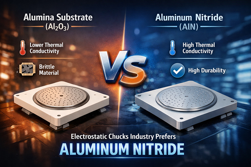 AlN Ceramic Substrates: Enabling Next-Gen Electrostatic Chucks
This article details the material properties forcing this change and provides a framework for ESC builders to evaluate and source the high-performance AlN substrates necessary to win in the advanced node market.
READ MORE >
AlN Ceramic Substrates: Enabling Next-Gen Electrostatic Chucks
This article details the material properties forcing this change and provides a framework for ESC builders to evaluate and source the high-performance AlN substrates necessary to win in the advanced node market.
READ MORE >
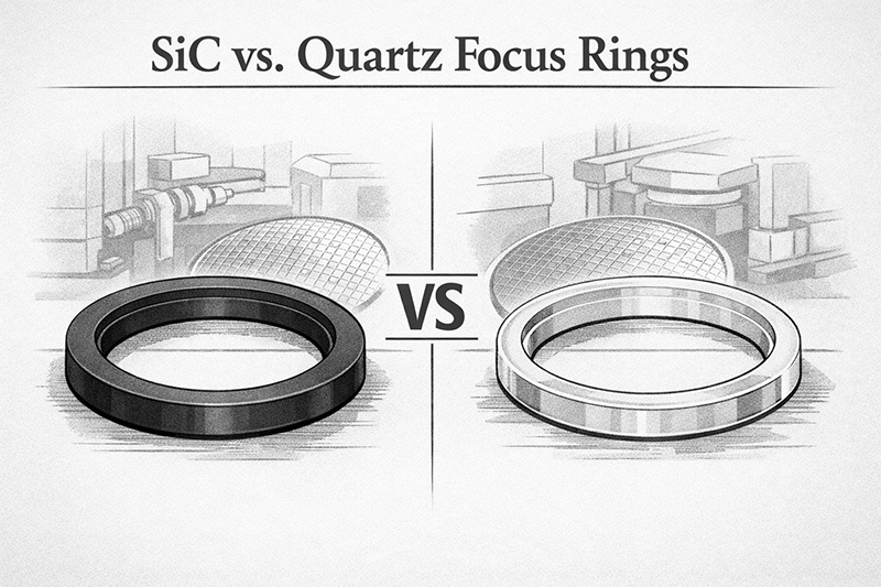 SiC vs. Quartz Focus Rings: A Cost and Performance Analysis for Advanced Etch
Quartz focus rings wear fast in advanced etch, hurting yield. Silicon Carbide (SiC) rings last 6-10x longer. Our TCO analysis shows how SiC's higher price lowers total cost. Get the selection guide and corrosion data.
READ MORE >
SiC vs. Quartz Focus Rings: A Cost and Performance Analysis for Advanced Etch
Quartz focus rings wear fast in advanced etch, hurting yield. Silicon Carbide (SiC) rings last 6-10x longer. Our TCO analysis shows how SiC's higher price lowers total cost. Get the selection guide and corrosion data.
READ MORE >
 How PBN Crucibles Ensure the Quality of GaN & SiC Epitaxial Materials
In the atomic-scale world of GaN HEMTs and SiC power devices, the vessel that holds the source materials is not just a container; it is the foundational determinant of epitaxial film purity. Trace contaminants from a crucible can incorporate as fatal defects. This article details why Pyrolytic Boron Nitride (PBN) has become the non-negotiable material for MOCVD and MBE components, examining its unique combination of ultra-high purity, thermal management, and non-wetting properties.
READ MORE >
How PBN Crucibles Ensure the Quality of GaN & SiC Epitaxial Materials
In the atomic-scale world of GaN HEMTs and SiC power devices, the vessel that holds the source materials is not just a container; it is the foundational determinant of epitaxial film purity. Trace contaminants from a crucible can incorporate as fatal defects. This article details why Pyrolytic Boron Nitride (PBN) has become the non-negotiable material for MOCVD and MBE components, examining its unique combination of ultra-high purity, thermal management, and non-wetting properties.
READ MORE >