


CY3453 CeO2 coated YSZ Substrate
- Catalog No. CY3453
- Substrate Material <110>, YSZ, 10x10x0.5 mm
- Surface finish One side polished
- Orientation <110>
- Epitaxial thin Film Composition CeO2
- Epitaxial Film Thickness 40 nm ± 10 nm
CY3453 CeO2 coated YSZ Substrate

CeO2 coated YSZ Substrate Description
CeO2 coated YSZ Substrate can be used as substrates in the nano field, scanning electron microscopy (SEM), atomic force microscopy (AFM), and other scanning probe microscope ranging, as well as cell culture, protein DNA microarrays, and reflectometers. The silicon wafer of this product is generally plated with a layer of CeO2 with a thickness of 40nm on one side.
CeO2 coated YSZ Substrate Specifications
|
Epitaxial thin Film Composition |
CeO2 |
|
Epitaxial Film Thickness |
40 nm ± 10 nm |
|
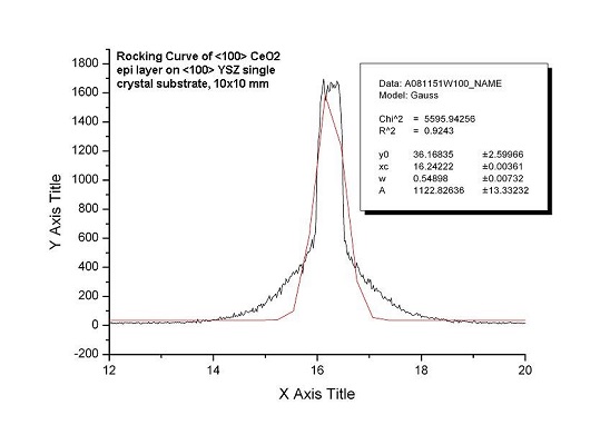
Epitaxial FWHM |
< 5 o |
|
Substrate |
<110>, YSZ, 10x10x0.5 mm |
|
Surface finish |
One side polished |
|
Orientation |
<110> |
CeO2 coated YSZ Substrate Applications
Widely used as substrates in the nano field, scanning electron microscopy (SEM), atomic force microscopy (AFM), and other scanning probe microscope ranging, as well as cell culture, protein DNA microarrays, and reflectometers.
CeO2 coated YSZ Substrate Packaging
Our CeO2 coated YSZ Substrate is carefully handled during storage and transportation to preserve the quality of our product in its original condition.
Packing: in 1000 class clean room with plastic bag
-
Attachment (Optional)
No file chosen


 Stabilized Zirconia Tube")